mbed addressbus, databus and controlbus
The mbed includes a very broad range of integrated peripherals:
- Ethernet, USB
- SPI, I2C, UART, CAN
- GPIO, PWM, ADC, DAC
However, in some cases you need to hook up devices that require a parallel 'bus' connection. This often includes a databus (8 bit), an addressbus (several bits) and some controlsignals like RD*, WR*, Reset and Chip Select. An example of such a device is a (legacy) LCD controller or a UART. Rather than use up the limited set of mbed portpins and loose all the available special functions that are provided on these pins, it may be possible in some cases to use a so-called port expander. A good example of a port expander for I2C is the PCF8574. Multiple PCF8574 devices can be connected by using the mbed I2C bus (SDA and SCL).
Given the fact that in many cases some protective buffering of mbed is preferred anyhow, the combination of the I2C bus and a number of low-cost I2C port expanders has other advantages too:
- Simplified level conversion: only the two I2C signals SDA and SCL need to be converted from 3.3V to 5V levels. The PCF8574 has 5V TTL output levels that can be easily adjusted to 5V CMOS levels by a simple pull-up resistor.
- Protective buffering provided by the 8 bit port expanders
- Easy to expand the bus in future (up to 16 PCF8574 and PCF8574A devices per I2C bus)
The I2C bus is well supported by the mbed libraries. The disadvantage of the approach using the I2C serial bus (typically 100Kbit/s, max 400Kbit/s) over a fully parallel bus is a slower update rate. However, that should not be a problem in many cases which need only a relatively low rate of data exchange (e.g. keyboard entries and displayresponses). The update rate issue has been further reduced by directly using a small number of peripheral pins for the controlbus (Read, Write etc). These signals are protected and level converted from mbed 3V3 to 5V TTL by a separate buffer device (SN74HCT244). The TTL levels may be input to mbed without adjustment to 3V3 since all LPC1768 inputs are 5V tolerant.
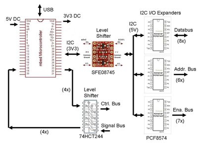
The blockdiagram is shown below.

In this setup we have
- databus (8 bit, I/O)
- addressbus (6 bit, Output)
- enablebus (7 bit, Output)
- controlbus (4 bit Output, 4 bit Input)
The controlbus inputs may be used for Interrups, busy signals etc. Level translation for I2C is provided by a Sparkfun module SFE08745.
A typical Write interaction between mbed and a display device on the bus is as follows:
Controlbus:
- WR* and RD* should be de-activated: Set to logic High level
- Optionally set DTR* High and CDBUF* Low to activate databus buffer for Write operation
Addressbus (I2C interaction):
- Set Addresslines A0-A7 to the proper address
Enablebus (I2C interaction):
- Set CSDISP* to Low, thus selecting the display
Databus (I2C interaction):
- Set D0-D7 to output the proper databyte
Controlbus:
- WR* activated: Set to logic Low level
- WR* de-activated: Set to logic High level. This concludes the Write operation
Enablebus (I2C interaction):
- Set CSDISP* to High, de-selecting the display
Controlbus:
- Optionally set CDBUF* to High to disable the databus buffer again.
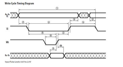
This results in the following WR sequence on the mbed bus:

Software has been developed to allow easy use of the parallel bus. For example:
void write(uint8_t address, CS_Pin device, uint8_t data)
{
//    // Switch databus buffer to outputs (note: this is the default state)
//    controlbus.busdir(WRITE);
//    // Switch databus to outputs
//    databus.busdir(WRITE);

    // Write out the address on to the addressbus and wait
    addressbus.write(address);
    wait_ms(DEVICE_WAIT_MS);

    // Set CE low and wait
    enablebus.chipselect(device, LOW);
    wait_ms(DEVICE_WAIT_MS);

    // Write data to the databus
    databus.write(data);
    wait_ms(DEVICE_WAIT_MS);

    // Set WR low, wait, then set high and wait
    controlbus.WR(LOW);
    wait_ms(DEVICE_WAIT_MS);
    controlbus.WR(HIGH);
    wait_ms(DEVICE_WAIT_MS);

    // Set CE high and wait
    enablebus.chipselect(device, HIGH);
    wait_ms(DEVICE_WAIT_MS);

//    // Switch databus back to inputs
//    databus.busdir(READ);
//    // Switch databus buffer back to inputs
//    controlbus.busdir(READ);

//    // Set address lines all high to minimise power through pullups
//    addressbus.write(0xFF);
}
In your own application you can develop a Class for each specific slave device and include modified versions of the 'read' and 'write' functions as 'private' member functions. This allows you to hardcode the device CS_pin signals, define specific delays when needed, change the sequence of CS, WR etc or mask out certain address or databits when they are not used in a particular case.
The libraries and example code can be found here [http://mbed.org/users/wim/programs/mbed_bus/lwtorn].
An example of how you may use this parallel bus to control a smart alphanumeric display can be found here http://mbed.org/users/wim/notebook/smart-alphanumeric-displays/
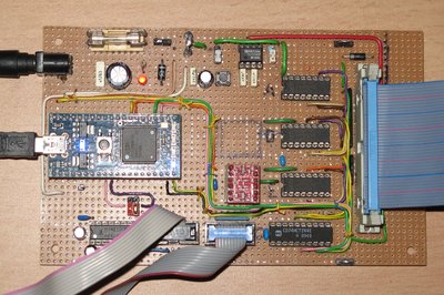
The mbed and the bus expander hardware is shown in the picture below. Note the 3 PCF8574 devices on the right hand side next to the flatcable connector.

Please log in to post comments.
